
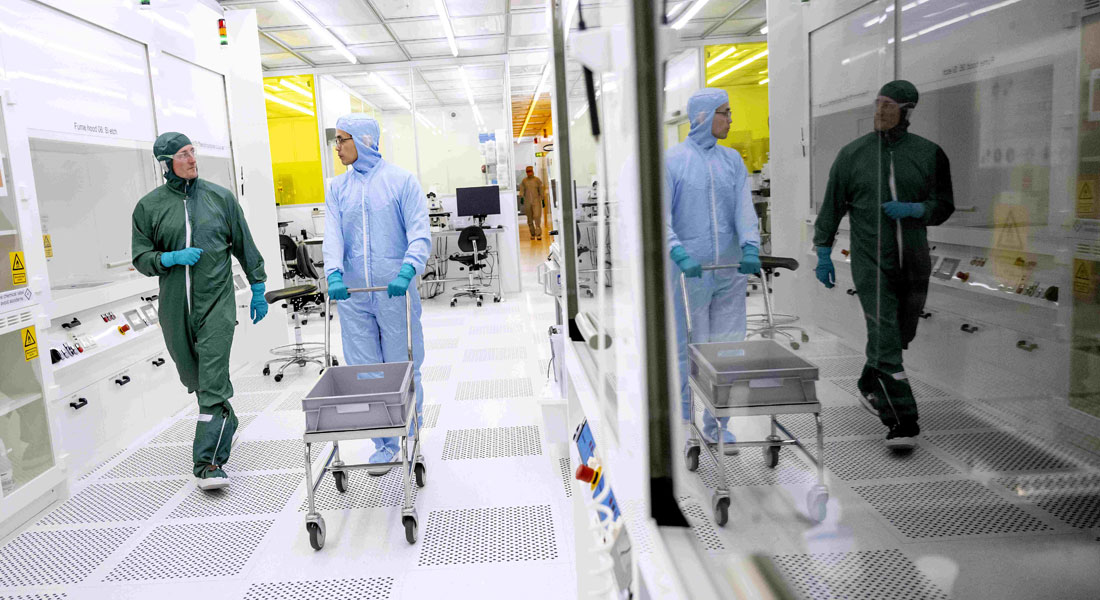
Quantum Material Fabrication
Cleanroom facilities with more than 150 state-of-the-art tools and equipment, ranging from atomic scale resolution transmission electron microscopes to a deep UV lithography stepper tool used for commercial chip production. Equipment for handling and bonding.
Multiple material systems;
- Processing of silicon as well as III-V materials, deposition of a wide range of materials using ALD (atomic layer deposition), PECVD (plasma enhanced vapor deposition), LPCVD (low pressure chemical vapor deposition), PVD (physical vapor deposition), MOVPE (metal organic vapor phase epitaxy
- Molecular Beam Epitaxy (MBE) ultra-high vacuum system for growth of III-V semiconductor compounds and in-situ hybridization with superconductors
For detailed information on capabilities and access, contact us or explore the test sites by yourself:
- Metrology Development
- Measurement standards and
- Calibration
- Metrology experts
 1350m2 Cleanroom (ISO 4)
- Electron Microscopes and Electron Beam Lithography (SEM(TEM/EBL)
- Optical Testbeds
- Supports up to 6” wafer fab
- ISO 9001 certified
- Process and microscopy specialists
- Optical characterization
- Ion traps
- Cold atoms
- Laser cooling facilities
- Specialists available within lasers/optics/photonics

 Cleanroom (ISO 7)
- Electron Microscopes and Electron Beam Lithography (SEM(TEM/EBL)
- Electrical and Optical Characterization
- Electrical and Mechanical Workshop
- Agile with fast feedback, ideal for small chips
- Process and microscopy specialists
- 3D imaging using x-rays and neutrons.